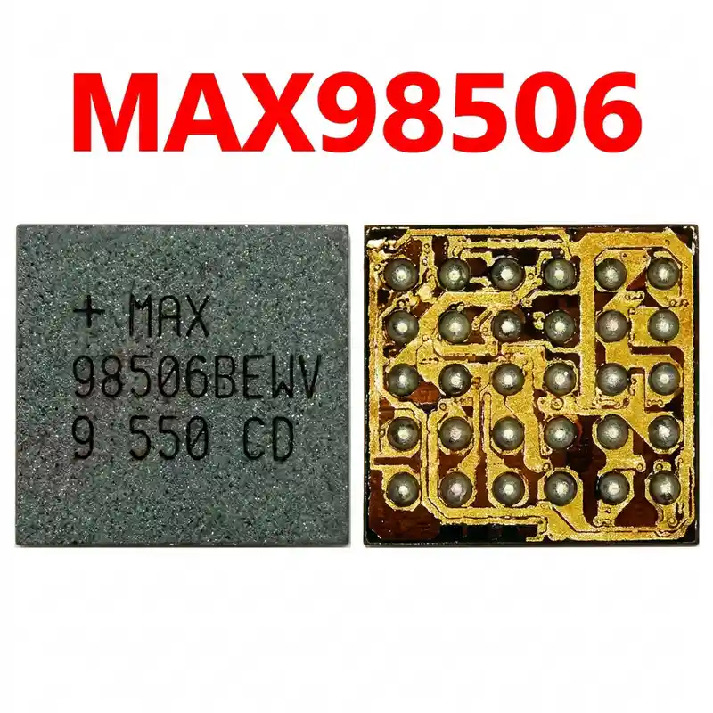
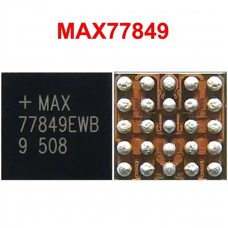
MAX20328B IC
As low as
Rs 0.00
Worldwide shipping · Cash on Delivery
Product Details
--------------------------------------------------------------------------------
SECTION 1: INTERNAL ARCHITECTURE & SWITCH TOPOLOGY
--------------------------------------------------------------------------------
1. Functional Blocks:
- Ultra-Low Resistance Audio Switches: Bidirectional analog switches supporting true negative swing down to -3V without external AC coupling capacitors.
- Dual-Channel Over-Voltage Lockout (OVLO): Continuously monitors SBU1 / SBU2 lines; automatically disconnects internal sensitive codec lines within 60ns if voltage exceeds safe threshold (~4.8V).
- Microphone & Ground Sense Routing: Automatically switches microphone and audio ground connections to support both CTIA and OMTP pinout configurations.
- Low-Distortion / Low-Noise Audio Engine: Integrated shunt switches eliminate audible "pop and click" transients when plugging in or unplugging earphones.
- I2C Control Interface: Serial control bus for mode configuration, interrupt status reading, and fault diagnostics.
--------------------------------------------------------------------------------
SECTION 2: STEP-BY-STEP MULTIMETER TESTING & DIAGNOSTICS
--------------------------------------------------------------------------------
1. Cold Resistance Testing (Diode Mode Readings - RED probe to GND, BLACK probe on test points):
- USB-C Connector SBU1 and SBU2 Pins (Test points / series components from sub-board flex):
* Normal Reading: ~480 mV to 620 mV (Both lines must show balanced values within ±15 mV).
* Short Circuit Fault: 0.000V indicates blown internal OVP clamp inside MAX20328B.
* Open Circuit (OL): Indicates burned input switch path or cracked solder ball.
- Audio Codec Output Lines (Left / Right / Mic lines towards CPU/PMIC):
* Normal Reading: ~500 mV to 680 mV.
- VDD_1P8 Logic Supply Capacitor:
* Normal Reading: ~420 mV to 550 mV.
- I2C Bus Lines (SDA / SCL):
* Normal Reading: ~450 mV to 560 mV.
2. Hot Voltage Testing (Board Powered ON with USB-C Earphones Connected):
- Measure VDD Logic Rail: Must read steady +1.8V DC.
- Plug in Type-C earphones:
* Measure SBU1/SBU2 lines: Bias voltage (~1.8V - 2.8V for mic) should appear. If 0V and phone does not display headphone icon in status bar, MAX20328B is not switching or is damaged.
--------------------------------------------------------------------------------
SECTION 3: DESOLDERING, REBALLING & REWORK SPECIFICATIONS
--------------------------------------------------------------------------------
1. Safe Removal:
- Samsung S10/S20 boards are multi-layer and dense. Shield nearby display connectors, camera sockets, and main PMIC with heat-reflective Kapton tape and thick aluminum shield.
- Apply a drop of quality tacky flux (Amtech NC-559 or Relife RL-422) around MAX20328B.
- Hot Air Settings: 330°C - 340°C with 20% - 25% airflow.
- Heat in a steady circular motion for 10–12 seconds until all 25 micro BGA balls liquefy; lift vertically with fine-tip tweezers.
2. PCB Pad Preparation:
- Apply 183°C leaded solder wire (Sn63/Pb37) to the 25 motherboard pads at 300°C using a micro-conical or fine-chisel tip to soften lead-free factory solder.
- Gently sweep flat with 0.6mm desoldering braid without applying downward pressure (pads are microscopic 0.4mm pitch).
- Clean the area thoroughly with 99.9% pure Isopropyl Alcohol (IPA) and inspect under microscope for any pad bridging.
3. Reballing & Installation of New MAX20328B:
- Use a dedicated Samsung S10/Note 10 audio/USB BGA stencil (Amaoe SAM series, 0.10mm or 0.12mm thickness).
- Apply 183°C solder paste smoothly; heat with hot air at 250°C to form uniform micro-balls.
- Apply a micro-thin layer of tacky flux on the cleaned motherboard pads.
- Align Pin 1 corner index dot precisely with the white silkscreen dot on the motherboard.
- Solder with hot air at 310°C - 320°C with low airflow (15% - 20%) to prevent air pressure from displacing the tiny chip.
- Allow natural cooling for 2 minutes, clean with IPA, connect the charging sub-board, and verify clear Type-C headphone detection, microphone input, and fast charging.
You may also like