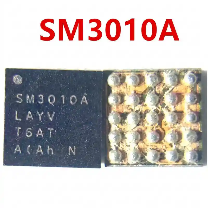
S5289 IC
As low as
Rs 300.00
Worldwide shipping · Cash on Delivery
Product Details
====================================================================================================
SAMSUNG S5289 DETAILED TECHNICAL GUIDE, USAGE & HARDWARE REWORK
====================================================================================================
1. FUNCTIONAL ARCHITECTURE & BOARD WORKING PRINCIPLE:
----------------------------------------------------------------------------------------------------
- Auxiliary Power Management & Sub-PMIC Role:
* The S5289 is a specialized secondary power management IC designed to handle localized multi-rail
voltage regulation for high-load peripheral modules, including optical camera mechanisms, sensors,
and secondary display/processor domains.
* In complex mechanical architectures (such as Samsung Galaxy A80 SM-A805F with motorized rotating
camera assembly), S5289 provides the dedicated regulated high-current power stages for drive motors,
stepper controllers, and high-resolution camera sensor VDD/AVDD lines.
- Low-Noise Precision LDO Regulators:
* Integrates multi-channel ultra-low-dropout (LDO) regulators generating clean analog power rails
(1.2V, 1.8V, 2.8V, and 3.3V) for image sensors, hall-effect position sensors, and secondary logic.
- Power Sequence Synchronization:
* Interfaces with the primary system PMIC via dedicated I2C/SPMI control lines, coordinating the power-on
and standby power-saving states when motorized camera or auxiliary peripherals are engaged.
2. COMPATIBLE SMARTPHONE PLATFORMS:
----------------------------------------------------------------------------------------------------
- Samsung Galaxy Series:
* Samsung Galaxy A80 (SM-A805F / SM-A8050 motorized rotating camera flagship)
- Vivo Series (Powered by Samsung Exynos Architecture):
* Vivo X30 / Vivo X30 Pro 5G (Exynos 980 platform)
- Selected Android platforms using Samsung System LSI auxiliary PMIC configurations.
3. BOARD-LEVEL FAULT SYMPTOMS:
----------------------------------------------------------------------------------------------------
- Motorized Camera Failure / Slider Stuck (Samsung A80 Specific):
* Switching to selfie mode causes camera mechanism to stall, make clicking noises, or display
"Camera failed" error on screen due to missing motor drive voltages from S5289.
- Dead Device / Low Current Boot Loop (0.02A–0.06A Stuck Current on DC Supply):
* S5289 internal regulator failure halts system boot-up handshake, leaving the phone stuck at low
current draw on the bench DC power supply.
- Severe Motherboard Hotspot & Standby Battery Drain:
* Internal short in one of the LDO stages causes S5289 to run boiling hot even when the screen is off,
draining the battery within a couple of hours.
- Primary Line Short Circuit (V_SYS / V_BAT Short to GND):
* Punctured input FET clamps the main battery bus to 0.000V in diode mode, tripping the DC power supply.
4. STEP-BY-STEP MULTIMETER TESTING & DIAGNOSTICS:
----------------------------------------------------------------------------------------------------
A. Cold Testing (Diode Mode Check - Board Powered Off, Battery Disconnected):
1. Connect Multimeter RED probe to PCB Ground (GND shield), probe with BLACK probe:
- Main Power Input Bypass Capacitors around S5289: Normal ~360mV – 460mV (0.000V = dead short).
- Auxiliary Output LDO Filter Capacitors: Normal ~420mV – 580mV across all peripheral lines.
- I2C Control Bus (SCL / SDA Lines): Normal ~450mV – 550mV (must read balanced).
2. Short-Circuit Thermal Isolation:
- If input rail reads 0.000V, inject 3.8V DC (limited to 1.5A). Inspect with thermal camera:
if S5289 lights up white-hot, remove the IC.
B. Live Operating Voltage Check (Hot Testing):
1. Power up the board using bench DC supply:
- Verify input pins receive steady 3.8V – 4.2V DC.
- Trigger camera application / selfie mode:
* Output filter capacitors must activate and deliver stable 2.8V and 3.3V DC to the camera
connector and drive circuitry.
* If input voltage is present but outputs collapse to 0V upon activation, replace S5289.
5. SOLDERING, REBALLING & REWORK SPECIFICATIONS:
----------------------------------------------------------------------------------------------------
- Thermal Protection & Surrounding Component Safety:
* S5289 is located near high-density flex connectors and shielded processing components.
* Always mask neighboring plastic FPC connectors and sensitive ICs with Kapton tape and copper coins.
- IC Removal:
* Apply premium non-corrosive RMA BGA tacky flux around the perimeter of S5289.
* Hot air rework station settings: 315°C – 325°C, airflow 30% – 35% with a fine precision nozzle.
* Heat evenly in small circles for 25–35 seconds. When solder balls liquefy, lift chip vertically.
- PCB Pad Cleanup:
* Apply 183°C (Sn63/Pb37) leaded solder alloy to lower pad alloy melting threshold.
* Flatten pad matrix completely using fine copper desoldering braid with soldering iron set to 285°C – 295°C.
* Clean residue with 99% Isopropyl Alcohol (IPA); inspect all pads under high microscope magnification.
- Reballing Procedure:
* Use a universal 0.12mm BGA stencil matching the S5289 footprint.
* Spread 183°C leaded solder paste smoothly across all apertures with a flexible scraper.
* Reflow gently at 270°C – 280°C with low airflow (20%) until uniform solder spheres form.
- Alignment & Installation:
* Spread a micro-thin layer of tacky BGA flux onto PCB pads.
* Align Pin 1 dot on S5289 with motherboard silkscreen orientation marking.
* Reflow at 305°C – 315°C with 30% airflow; watch chip gently pull into center via solder surface tension.
* Allow logic board to cool naturally for 3–5 minutes before connecting battery or testing.
====================================================================================================
You may also like