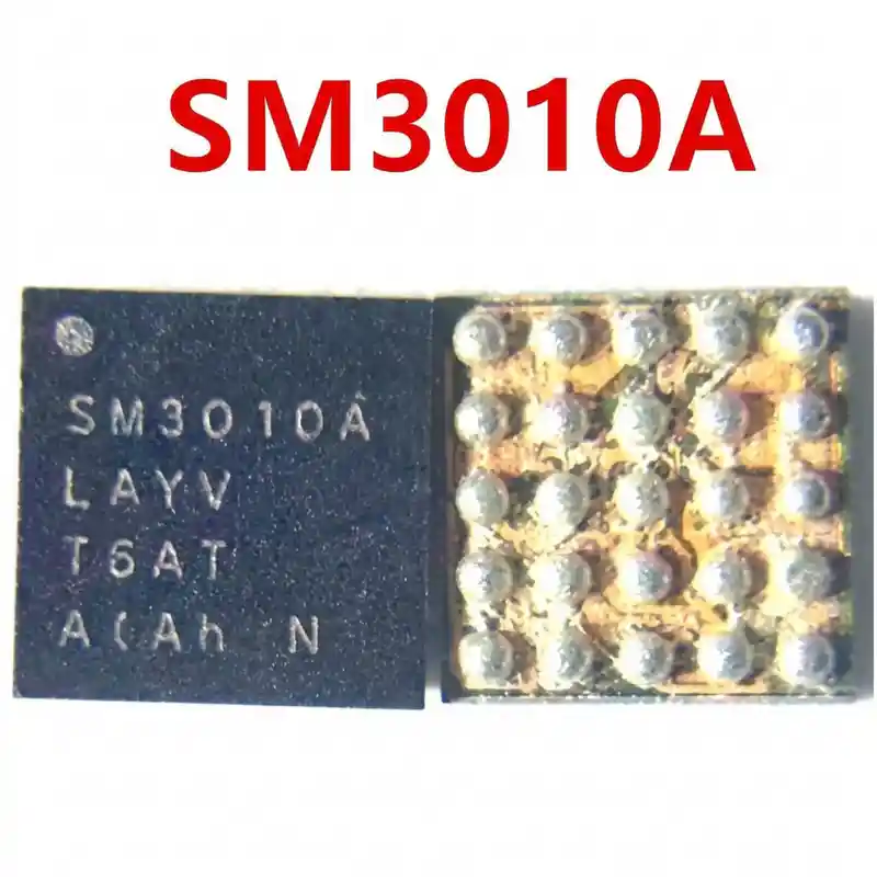
SM5713S IC
As low as
Rs 200.00
Worldwide shipping · Cash on Delivery
Product Details
====================================================================================================
SILICON MITUS SM5713S DETAILED TECHNICAL GUIDE, USAGE & HARDWARE REWORK
====================================================================================================
1. FUNCTIONAL ARCHITECTURE & BOARD WORKING PRINCIPLE:
----------------------------------------------------------------------------------------------------
- Sub-PMIC & Switching Fast Battery Charger:
* The SM5713S is a high-integration secondary PMIC designed to manage high-efficiency synchronous
step-down battery charging from 5V and 9V USB Type-C power sources (supporting Samsung Adaptive Fast
Charging - AFC up to 15W–25W).
* Controls constant current (CC) and constant voltage (CV) battery charging curves while monitoring
internal and battery thermistor (NTC) temperatures.
- Main System Power Rail Generation (V_SYS / VPH_PWR):
* Converts incoming USB power and battery voltage into the main system power bus (3.7V – 4.2V DC),
distributing power across the motherboard to the primary PMIC (e.g., Shannon or Qualcomm PMIC),
RF power amplifiers, and audio subsystems.
- Auxiliary Power Stages & LDO Regulators:
* Contains integrated linear LDO regulators supplying clean power to optical fingerprint sensors,
display interface logic, and camera sensor analog rails.
- Flash & Peripheral Drivers:
* Integrated high-current strobe driver for rear camera flash and flashlight torch.
* USB Type-C interface logic and 5.0V reverse step-up boost converter for USB OTG accessory support.
2. COMPATIBLE SMARTPHONE PLATFORMS:
----------------------------------------------------------------------------------------------------
- Samsung Galaxy A-Series (High Failure Rate in Repair Centers):
* Galaxy A70 (SM-A705F, SM-A705FN, SM-A705GM, SM-A7050 - Native SM5713S Configuration)
* Galaxy A50 (SM-A505F, SM-A505FN, SM-A505G)
* Galaxy A60 (SM-A606F, SM-A6060)
* Galaxy A40 (SM-A405F, SM-A405FN)
* Galaxy A8s (SM-G8870)
- Samsung Galaxy Flagship Tier (Secondary Power & Charging Tier):
* Galaxy S10 / Galaxy S10+ / Galaxy S10e (Exynos variants)
* Galaxy S10 Lite / Note 10 Lite
- Selected Samsung Galaxy M-Series devices (M30s, M31).
3. BOARD-LEVEL FAULT SYMPTOMS:
----------------------------------------------------------------------------------------------------
- Completely Dead Phone (0.000A or 0.02A–0.05A Stuck Draw on DC Power Supply):
* Failure of internal switching buck circuit prevents V_SYS generation. Main PMIC and CPU receive 0V.
- Fake Charging (Charging Lightning Bolt Shows on LCD, but Battery Drains):
* Device indicates charging on screen, but USB ammeter reads 0.00A–0.15A; battery slowly loses charge.
- "Charging Paused / Yellow Temperature Triangle" Warning on Boot:
* Internal battery thermistor ADC lines inside SM5713S become damaged by voltage spikes or water
ingress, triggering false overheating warnings and halting charging.
- Severe Motherboard Hotspot & Rapid Overnight Battery Drain:
* Internal breakdown in switching MOSFET array causes SM5713S to run burning hot (60°C–90°C) even
when the device is in standby or powered off.
- V_SYS / Battery Rail Dead Short to Ground (0.000V in Diode Mode):
* Punctured high-side buck MOSFET shorts the main system line directly to Ground, causing bench DC
power supply to trip overcurrent protection instantly on battery connection.
4. STEP-BY-STEP MULTIMETER TESTING & DIAGNOSTICS:
----------------------------------------------------------------------------------------------------
A. Cold Testing (Diode Mode Check - Board Powered Off, Battery Disconnected):
1. Place Multimeter in Diode Mode. Connect RED probe to Motherboard Ground (GND shield):
- VBUS Input Filter Capacitors (near Type-C flex connector): Normal ~450mV – 560mV (0.000V = dead short).
- Battery Connector Positive Terminal (VBAT): Normal ~400mV – 480mV.
- V_SYS Inductor (large switching coil next to SM5713S): Normal ~350mV – 450mV (0.000V = dead short).
- Bootstrap Capacitor (BST): Measure across both terminals; must show high impedance (no short).
- I2C Control Bus (SCL / SDA to CPU): Normal ~450mV – 550mV (balanced readings on both).
2. Short-Circuit Thermal Detection:
- If V_SYS reads 0.000V, inject 3.8V DC (limited to 2.0A) onto the inductor.
Observe under thermal camera: if SM5713S illuminates bright white instantly, desolder the chip.
B. Live Operating Voltage Check (Hot Testing):
1. Connect 5V / 9V USB Type-C charger:
- VBUS Input Capacitor: Must measure steady 5.0V – 5.2V DC (or 9.0V in AFC fast-charge mode).
- V_SYS Inductor: Must output steady 3.7V – 4.2V DC (even with battery disconnected).
- Battery Terminal Pins: Must show pulsed 3.7V – 4.35V DC charging voltage.
- If 5V arrives at VBUS but V_SYS inductor measures 0V or pulses continuously, SM5713S has failed.
5. SOLDERING, REBALLING & REWORK SPECIFICATIONS:
----------------------------------------------------------------------------------------------------
- Thermal Protection & Surrounding Component Safety:
* On Galaxy A70/A50, SM5713S is situated under a soldered metal shield close to the CPU and UFS/eMMC.
* Always mask the neighboring processor and memory chips with thick Kapton thermal tape and copper coins.
- IC Removal:
* Dispense high-grade non-corrosive RMA BGA tacky flux around the perimeter of SM5713S.
* Hot air rework parameters: 315°C – 330°C, airflow 35% – 40% with a medium precision nozzle.
* Heat in even circular motions for 30–40 seconds. When solder balls liquefy, lift chip vertically.
- PCB Pad Cleanup:
* Apply 183°C (Sn63/Pb37) leaded solder to logic board footprint to dilute factory high-melt unleaded alloy.
* Flatten pad matrix completely using fine copper desoldering braid with soldering iron set to 285°C – 295°C.
* Clean residue thoroughly with 99% Isopropyl Alcohol (IPA); inspect pads under microscope for any lifted pads.
- Reballing Procedure:
* Use a dedicated or universal 0.12mm BGA stencil matching the SM5713 / SM5713S footprint.
* Spread 183°C leaded solder paste smoothly across all apertures with a flexible scraper.
* Reflow gently at 270°C – 280°C with low airflow (20%) until uniform solder spheres form.
- Alignment & Installation:
* Spread a micro-thin layer of tacky BGA flux onto PCB pads.
* Align Pin 1 dot on SM5713S with motherboard silkscreen corner indicator.
* Reflow at 305°C – 315°C with 35% airflow; observe chip self-center on molten solder surface tension.
* Allow logic board to cool naturally for 3–5 minutes before connecting DC power or battery.
====================================================================================================
You may also like