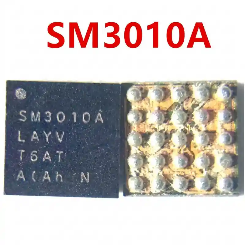
SGM3838 IC
As low as
Rs 200.00
Worldwide shipping · Cash on Delivery
Product Details
====================================================================================================
SG MICRO SGM3838 DETAILED TECHNICAL GUIDE, USAGE & HARDWARE REWORK
====================================================================================================
1. FUNCTIONAL ARCHITECTURE & BOARD WORKING PRINCIPLE:
----------------------------------------------------------------------------------------------------
- Dedicated AMOLED Power Generation:
* AMOLED screens do not have an external LED backlight strip; each sub-pixel emits its own light.
* To power millions of OLED pixels and display drivers, the SGM3838 produces 3 distinct synchronized rails:
1. VO1 - Synchronous Boost Converter (ELVDD):
- Positive pixel supply delivering +4.6V (programmable 4.6V to 5.0V in 100mV steps) at up to 700mA.
- Includes Path Loss Compensation (FBS pin) to sense voltage drop right at the display FPC connector.
2. VO2 - Dual-Phase Inverting Buck-Boost Converter (ELVSS):
- Negative cathode supply delivering -3.0V (programmable -6.0V to -0.8V in 100mV steps) at up to 700mA.
3. VO3 - Synchronous Auxiliary Boost Converter (AVDD):
- Analog bias supply delivering +7.3V (programmable 5.5V to 7.9V in 100mV steps) at up to 150mA.
- Digital SWIRE (Single-Wire) Bus Control:
* Receives high-speed digital pulses from the application processor on the SWIRE pin to dynamically
adjust ELVDD/ELVSS levels according to screen brightness, DC-dimming, and refresh rate modes (60Hz/120Hz).
- Hardware Protection Features:
* Bi-directional input/output isolation (prevents battery discharge when screen is off).
* Fast Short-Circuit Protection (SCP) and Overload Protection (OLP) with 0.71ms fault latch time.
* Precision thermal shutdown preventing silicon thermal damage.
2. COMPATIBLE SMARTPHONE PLATFORMS:
----------------------------------------------------------------------------------------------------
- Huawei Series:
* Huawei Nova 9 / Nova 9 Pro (Snapdragon 778G 4G)
* Huawei Nova 8 / Nova 8 Pro
- Honor Series:
* Honor 50 / Honor 50 Pro (Snapdragon 778G)
* Honor 60 / Honor 60 Pro
- Xiaomi / Redmi Series:
* Selected Redmi Note and Xiaomi models utilizing 120Hz curved or flat AMOLED display panels.
- Oppo / Vivo Series:
* Mid-range AMOLED smartphones requiring discrete triple-output display bias power solutions.
3. BOARD-LEVEL FAULT SYMPTOMS:
----------------------------------------------------------------------------------------------------
- Completely Blank / Pitch Black Screen (Phone Fully Powered On):
* Handset vibrates on startup, sounds boot ringtones, receives calls and WhatsApp notifications,
touch screen may respond to swipes, but display shows zero graphics (missing ELVDD +4.6V or ELVSS -3.0V).
- Screen Flashes Once and Goes Black on Boot:
* Display lights up for half a second showing vendor splash logo, then instantly turns pitch black.
Caused by SGM3838 tripping Overload Protection (OLP) due to cracked inductor or shorted filter cap.
- Dim Screen / Severe Color Distortion / Green Tint:
* ELVSS negative rail fails to reach -3.0V (stuck at 0V or fluctuating), causing OLED pixels to lose
proper black levels, producing washed-out or greenish hue across the display panel.
- VPH_PWR / Battery Rail Short Circuit:
* Blown internal switching FET inside SGM3838 shorts the main system line directly to Ground (0.000V),
causing the phone to become completely dead and DC bench power supply to trip instantly.
- Extreme Localized Overheating:
* SGM3838 gets scorching hot near the display FPC connector within seconds of pressing the power key.
4. STEP-BY-STEP MULTIMETER TESTING & DIAGNOSTICS:
----------------------------------------------------------------------------------------------------
A. Cold Testing (Diode Mode Check - Board Powered Off, Battery Disconnected):
1. Place Multimeter in Diode Mode. Connect RED probe to Motherboard Ground (GND shield):
- VIN Input Filtering Capacitors (from VPH_PWR/VBAT): Normal ~360mV – 460mV (0.000V = dead short).
- VO1 (ELVDD +4.6V) Output Capacitors: Normal ~420mV – 520mV.
- VO2 (ELVSS -3.0V) Output Capacitors: Normal ~480mV – 580mV (must NOT read 0.000V).
- VO3 (AVDD +7.3V) Output Capacitors: Normal ~450mV – 550mV.
- SWIRE Control Line to CPU: Normal ~450mV – 600mV.
2. Inductor & Boost Continuity:
- Inspect the external switching inductors around SGM3838; verify they are not cracked or open.
B. Live Operating Voltage Check (Hot Testing - Display Connected, Board Powered On):
1. Connect DC bench power supply and trigger power-on with display connected:
- VIN: Must measure steady 3.7V – 4.2V DC.
- VO1 Inductor / Capacitor: Must measure +4.6V DC steady when screen turns on.
- VO2 Capacitor: Must measure -3.0V DC (negative voltage; black probe on cap, red on GND = +3.0V).
- VO3 Capacitor: Must measure +7.3V DC steady.
- If VIN is present but all three output rails are 0V, verify the SWIRE enable signal from CPU.
If SWIRE pulses on boot but outputs remain 0V, SGM3838 is defective.
5. SOLDERING, REBALLING & REWORK SPECIFICATIONS:
----------------------------------------------------------------------------------------------------
- High Sensitivity Bare Silicon Die (WLCSP-36):
* SGM3838 is an ultra-compact bare-silicon wafer package (2.5mm x 2.5mm). It is brittle and easily
chipped by metal tweezers. Always lift gently from underneath using thin, curved tweezers.
- IC Removal:
* Apply high-grade, non-corrosive RMA BGA tacky flux around the chip perimeter.
* Hot air rework station settings: 315°C – 330°C, airflow 30% – 35% with a fine precision nozzle.
* Heat evenly in smooth circular motion for 25–35 seconds. When all 36 solder balls liquefy, lift vertically.
- PCB Pad Cleanup:
* Add 183°C (Sn63/Pb37) leaded solder to dilute factory high-melt unleaded alloy.
* Clean pad matrix completely flat using fine copper desoldering braid and soldering iron set to 285°C – 295°C.
* Clean residue with 99% Isopropyl Alcohol (IPA); inspect all 36 pads under high microscope magnification.
- Reballing Procedure:
* Use a dedicated 0.12mm WLCSP-36 BGA stencil (0.4mm pitch) or universal AMOLED PMIC stencil.
* Squeegee 183°C leaded solder paste uniformly into all 36 apertures.
* Reflow gently at 270°C – 280°C with low airflow (20%) until uniform solder spheres form.
- Alignment & Installation:
* Spread an extremely thin, transparent film of tacky BGA flux onto PCB pads.
* Align Pin A1 index orientation dot precisely with motherboard silkscreen corner indicator.
* Reflow at 305°C – 315°C with 30% airflow; watch chip gently self-center on molten solder surface tension.
* Allow logic board to cool naturally for 3–5 minutes before connecting display and battery.
====================================================================================================
You may also like