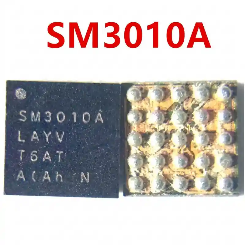
SC6601A IC
As low as
Rs 1000.00
Worldwide shipping · Cash on Delivery
Product Details
====================================================================================================
SOUTHCHIP SC6601A DETAILED TECHNICAL GUIDE, USAGE & HARDWARE REWORK
====================================================================================================
1. FUNCTIONAL ARCHITECTURE & BOARD WORKING PRINCIPLE:
----------------------------------------------------------------------------------------------------
- Battery Power Path Management:
* The SC6601A integrates low on-resistance power MOSFET switches that select dynamically between
USB charger power (VBUS) and direct battery power (VBAT) to feed the system.
* When the battery is fully drained, it isolates the battery, allowing the phone to boot immediately
from the USB charger power rail before sufficient charge is built up.
- High-Efficiency Switching Fast Charging:
* Controls step-down switching charging current into single-cell Li-ion batteries, supporting fast-charge
protocols with programmable charging current limits (up to 3.0A+).
- Integrated Reverse Protection & Safety Gate:
* Built-in Over-Voltage Protection (OVP), Over-Current Protection (OCP), reverse-blocking FETs
(preventing battery power from leaking back into the charging port), and thermal throttling.
- Digital Communication & Status Feedback:
* Communicates with the main application processor (MediaTek / Qualcomm / Unisoc platforms) via
I2C bus to report live charging current, battery temperature, and charging phase status.
2. COMPATIBLE SMARTPHONE PLATFORMS:
----------------------------------------------------------------------------------------------------
- Xiaomi / Redmi Series:
* Xiaomi Redmi 13 (4G edition)
* Xiaomi Poco M6
- Selected Recent Android Platforms:
* Contemporary budget and mid-range devices from Oppo, Vivo, Realme, Tecno, and Infinix that utilize
Southchip secondary charging architectures.
3. BOARD-LEVEL FAULT SYMPTOMS:
----------------------------------------------------------------------------------------------------
- Device Boots Only with Charger Plugged In (Does Not Turn On From Battery):
* Classic Southchip power-path failure: Phone turns on and works normally when connected to the USB
cable, but the moment the charger is removed, the phone instantly dies (internal battery switch open).
- Complete No-Charging / USB Unrecognized (0.00A Current Draw):
* Connecting a functional USB cable shows no charging indication or draws 0.00A on a USB ammeter.
- Fake Charging (Charging Animation Appears but Battery Percentage Drains):
* Phone displays lightning bolt icon on battery, but charging current remains under 0.10A; battery drains.
- VBUS Direct Short to Ground (0.000V in Diode Mode):
* Punctured input protection FET inside SC6601A causes the USB charger to trip overcurrent protection.
- Extreme Overheating on Motherboard:
* SC6601A becomes scalding hot to the touch immediately upon connecting the charging cable.
4. STEP-BY-STEP MULTIMETER TESTING & DIAGNOSTICS:
----------------------------------------------------------------------------------------------------
A. Cold Testing (Diode Mode Check - Board Powered Off, Battery Disconnected):
1. Place Multimeter in Diode Mode. Connect RED probe to Motherboard Ground (GND shield):
- VBUS Input Filter Capacitors: Normal ~450mV – 560mV (0.000V = dead short).
- Battery Output Terminal (VBAT connection line): Normal ~400mV – 480mV.
- System Power Bus (VSYS) Inductor/Capacitor: Normal ~350mV – 450mV.
- I2C Bus Pins (SCL / SDA): Normal ~450mV – 550mV (balanced readings on both).
2. Short-Circuit Isolation:
- If VBUS or VBAT reads 0.000V, inject voltage (3.8V for VBAT, 5.0V for VBUS) limited to 1.5A.
Inspect under thermal camera: if SC6601A glows brightly, desolder the IC.
B. Live Operating Voltage Check (Hot Testing):
1. Insert 5V USB charger cable:
- VBUS Input Capacitor: Must measure steady 5.0V – 5.2V DC.
- System Rail (VSYS): Must read steady 3.8V – 4.2V DC.
- Battery Terminal: Must show pulsating 3.7V – 4.35V DC charging voltage.
- If 5V arrives at input but system rail and battery terminal remain 0V, SC6601A has failed.
5. SOLDERING, REBALLING & REWORK SPECIFICATIONS:
----------------------------------------------------------------------------------------------------
- Package Fragility (Ultra-Compact WLCSP Bare Silicon):
* SC6601A is an unencapsulated bare-die chip; take care not to chip the corners or edges with tweezers.
- IC Removal:
* Dispense high-grade non-corrosive RMA BGA tacky flux around the perimeter of SC6601A.
* Hot air rework parameters: 310°C – 325°C, airflow 30% – 35% with a fine precision nozzle.
* Heat in even circular motions for 25–35 seconds. When solder balls liquefy, lift chip vertically.
- PCB Pad Cleanup:
* Apply 183°C (Sn63/Pb37) leaded solder to dilute factory high-melt unleaded alloy.
* Clean pad matrix completely flat using fine copper desoldering braid and soldering iron set to 285°C – 295°C.
* Clean residue with 99% Isopropyl Alcohol (IPA); inspect pads under microscope for any lifted traces.
- Reballing Procedure:
* Use a universal 0.12mm WLCSP/BGA stencil matching the SC6601A pad layout.
* Spread 183°C leaded solder paste smoothly across all apertures with a flexible scraper.
* Reflow gently at 270°C – 280°C with low airflow (20%) until uniform solder spheres form.
- Alignment & Installation:
* Spread a micro-thin layer of tacky BGA flux onto PCB pads.
* Align Pin 1 dot on SC6601A with motherboard silkscreen orientation marking.
* Reflow at 305°C – 315°C with 30% airflow; observe chip self-center on molten solder surface tension.
* Allow logic board to cool naturally for 3–5 minutes before connecting battery or charger.
====================================================================================================
You may also like